
Desert Online General Trading LLC
Dubai, United Arab Emirates
Desert Online General Trading LLC
Dubai, United Arab Emirates
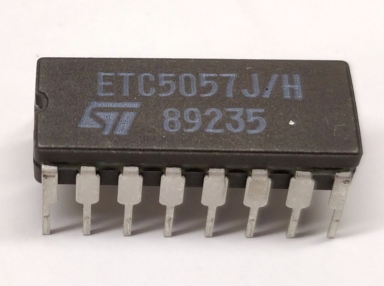
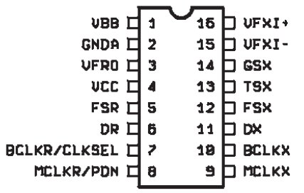
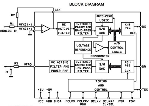

The ETC5057 family consists of a law monolithic PCM Codec/filters utilizing the a/d and d/a conversion architecture shown in the block diagram below, and a serial PCM Interface. The devices are fabricated using Doublepoly CMOS process. The Encode portion of each device consists of an input gain adjust amplifier, to active RC pre-filter which eliminates very high frequency noise prior to entering a switched-Capacitor band pass filter that rejects signal below 200 Hz and above 3400 Hz. Also included are car Zero circuitry and a companding coder which samples the filtered signal and encodes it in the companded a law or U?Law PCM format. The Decode portion of each device consists of an expanding decoder – which reconstructs the analog signal from the companded a law or U?Law Code, a low pass filter which corrects for the sin x/x response of the decoder output and rejects signals above 3400 Hz and is followed by a single ended power amplifier capable of driving low impedance loads. The devices require 1.536 MHz, 1.544 MHz, or 2048 MHz transmit and receive Master clocks, which may be asynchronous, bit clocks which may vary from 64 kHz to 2048 MHz transmit and receive, and transmit and receive frame sync pulses. Complete codec and filter ring system (device) including:Transmit high pass and low pass filtering.Receive Low Pass Filter with sin x/correction.Activerc noise filterU Lawor a Lawcompatiblecoderanddecoder.Internal precision voltage reference.Serial I/O Interface is built.Internal Auto zero circuitry.A law 16 pins (ETC5057FN, 20 pins)Meets or exceeds all D3/D4 and CCITT Specifications± 5 V OperationLow operating power – typi Cally 60mWPower-down Standby mode – typi Cally 3mWAutomatic power-downTTL or CMOS Compatible Digital interfacesMaximizes line interface card circuit density
Trustpilot
2 weeks ago
2 months ago